|
点击阅读英文原文
6 memory considerations for Cortex-M7-based IoT designs
Taking a closer look at the configurable memory aspects of Cortex-M7 microcontrollers.
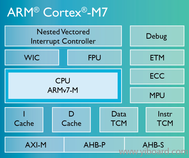
Tightly coupled memory (TCM) is a salient feature in the Cortex-M7 lineup as it boosts the MCU’s performance by offering single cycle access for the CPU and by securing the high-priority latency-critical requests from the peripherals.

The early MCU implementations based on the ARM’s M7 embedded processor core — like Atmel’s SAM E70 and S70 chips — have arrived in the market. So it’d be worthwhile to have a closer look at the configurable memory aspects of M7 microcontrollers and see how the TCMs enable the execution of deterministic code and fast transfer of real-time data at the full processor speed.
Here are some of the key findings regarding the advanced memory architecture of Cortex-M7 microcontrollers:
1. TCM is Configurable
First and foremost, the size of TCM is configurable. TCM, which is part of the physical memory map of the MCU, supports up to 16MB of tightly coupled memory. The configurability of the ARM Cortex-M7 core allows SoC architects to integrate a range of cache sizes. So that industrial and Internet of Things product developers can determine the amount of critical code and real-time data in TCM to meet the needs of the target application.
The Atmel | SMART Cortex-M7 architecture doesn’t specify what type of memory or how much memory should be provided; instead, it leaves these decisions to designers implementing M7 in a microcontroller as a venue for differentiation. Consequently, a flexible memory system can be optimized for performance, determinism and low latency, and thus can be tuned to specific application requirements.
2. Instruction TCM
Instruction TCM or ITCM implements critical code with deterministic execution for real-time processing applications such as audio encoding/decoding, audio processing and motor control. The use of standard memory will lead to delays due to cache misses and interrupts, and therefore will hamper the deterministic timing required for real-time response and seamless audio and video performance.
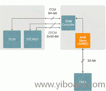
The deterministic critical software routines should be loaded in a 64-bit instruction memory port (ITCM) that supports dual-issue processor architecture and provide single-cycle access for the CPU to boost MCU performance. However, developers need to carefully calibrate the amount of code that need zero-wait execution performance to determine the amount of ITCM required in an MCU device.

The anatomy of TCM inside the M7 architecture.
3. Data TCM
Data TCM or DTCM is used in fast data processing tasks like 2D bar decoding and fingerprint and voice recognition. There are two data ports (DTCMs) that provide simultaneous and parallel 32-bit data accesses to real-time data. Both instruction TCM and data TCM — used for efficient access to on-chip Flash and external resources — must have the same size.
4. System RAM and TCM
System RAM, also known as general RAM, is employed for communications stacks related to networking, field buss, high-bandwidth bridging, USB, etc. It implements peripheral data buffers generally through direct memory access (DMA) engines and can be accessed by masters without CPU intervention.
Here, product developers must remember the memory access conflicts that arise from the concurrent data transfer to both CPU and DMA. So developers must set clear priorities for latency-critical requests from the peripherals and carefully plan latency-critical data transfers like the transfer of a USB descriptor or a slow data rate peripheral with a small local buffer. Access from the DMA and the caches are generally burst to consecutive addresses to optimize system performance.
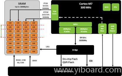
It’s worth noting that while system memory is logically separate from the TCM, microcontroller suppliers like Atmel are incorporating TCM and system RAM in a single SRAM block. That lets IoT developers share general-purpose tasks while splitting TCM and system RAM functions for specific use cases.

A single SRAM block for TCM and system memory allows higher flexibility and utilization.
5. TCM Loading
The Cortex-M7 uses a scattered RAM architecture to allow the MCU to maximize performance by having a dedicated RAM part for critical tasks and data transfer. The TCM might be loaded from a number of sources, and these sources aren’t specified in the M7 architecture. It’s left to the MCU designers whether there is a single DMA or several data loading points from various streams like USB and video.
It’s imperative that, during the software build, IoT product developers identify which code segments and data blocks are allocated to the TCM. This is done by embedding programs into the software and by applying linker settings so that software build appropriately places the code in memory allocation.
6. Why SRAM?
Flash memory can be attached to a TCM interface, but the Flash cannot run at the processor clock speed and will require caching. As a result, this will cause delays when cache misses occur, threatening the deterministic value proposition of the TCM technology.
DRAM technology is a theoretical choice but it’s cost prohibitive. That leaves SRAM as a viable candidate for fast, direct and uncached TCM access. SRAM can be easily embedded on a chip and permits random accesses at the speed of the processor. However, cost-per-bit of SRAM is higher than Flash and DRAM, which means it’s critical to keep the size of the TCM limited.
Atmel | SMART Cortex-M7 MCUs
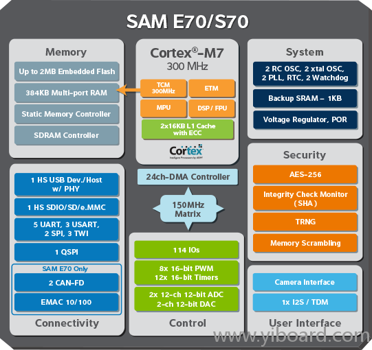
Take the case of Atmel’s SMART SAM E70, S70 and V70/71 microcontrollers that organize SRAM into four memory banks for TCM and System SRAM parts. The company has recently started shipping volume units of its SAM E70 and S70 families for the IoT and industrial markets, and claims that these MCUs provide 50 percent better performance than the closest competitor.

Atmel’s M7-based microcontrollers offer up to 384KB of embedded SRAM that is configurable as TCM or system memory for providing IoT designs with higher flexibility and utilization. For instance, E70 and S70 microcontrollers organize 384KB of embedded SRAM into four ports to limit memory access conflicts. These MCUs allocate 256KB of SRAM for TCM functions — 128 KB for ITCM and DTCM each — to deliver zero wait access at 300MHz processor speed, while the remaining 128KB of SRAM can be configured as system memory running at 150MHz.
However, the availability of an SRAM block organized in the form of a memory bank of 384KB means that both system SRAM and TCM can be used at the same time.The large on-chip SRAM of 384KB is also critical for many IoT devices, since it enables them to run multiple communication stacks and applications on the same MCU without adding external memory. That’s a significant value proposition in the IoT realm because avoiding external memories lowers the BOM cost, reduces the PCB footprint and eliminates the complexity in the high-speed PCB design.
|